New Nanoscale Process Created by UCSB Scientists Will Help Computers Run Faster and More Efficiently

Smaller. Faster. More efficient. These are the qualities that drive science and industry to create new nanoscale structures that will help to speed up computers.
Scientists at the University of California, Santa Barbara have made a major contribution to this field by designing a new nanotechnology that will ultimately help make computers smaller, faster, and more efficient. The new process is described in today's Science Express, the online version of the journal Science.
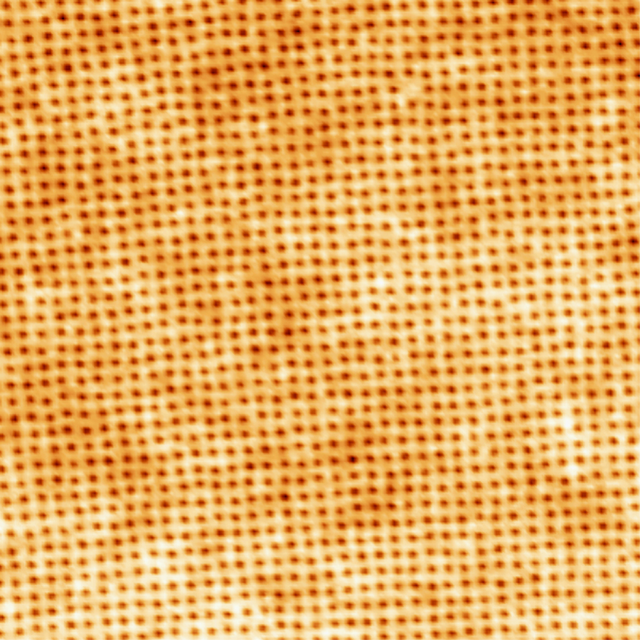
For the first time, the UCSB scientists have created a way to make square, nanoscale, chemical patterns –– from the bottom up ––that may be used in the manufacture of integrated circuit chips as early as 2011. It is called block co-polymer lithography.
Five leading manufacturers, including Intel and IBM, helped fund the research at UCSB, along with the National Science Foundation and other funders. The university has already applied for patents on the new methods developed here, and it will retain ownership.
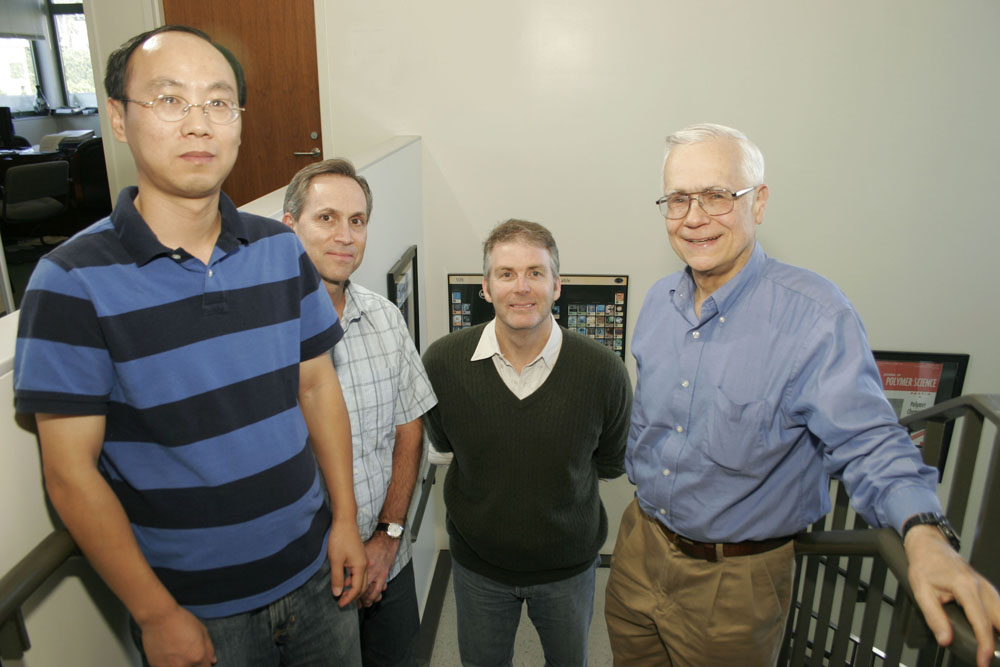
A multidisciplinary team led by Craig Hawker, materials professor and director of the Materials Research Laboratory at UCSB, with professors Glenn Fredrickson and Edward J.
Kramer, have developed a novel process for creating features on silicon wafers that are between five and 20 nanometers thick. (A nanometer is the thickness of one-thousandth of a human hair.)
Hawker explained that for the future we need more powerful microprocessors that use less energy. "If you can shrink all these things down, you get both," he said "You get power and energy efficiency in one package."
He said that the industry is up against Moore's law, a trend that Gordon Moore, Intel co-founder, first described in 1965 in which the power of the microprocessor doubles every 18 months. "One of the problems is that the industry is now running into physical limitations," said Hawker. "You can't shrink things down any more with the current technology." One of the ways that microprocessors are made is by using a top-down technique called photolithography, which involves shining light onto the surface of a silicon wafer, and making patterns. He explained that the size of the wavelength of light is becoming a limiting factor, and so his team has invented a new way of creating smaller patterns.
"We've come up with this new blending approach, called block co-polymer lithography, or BCP," said Hawker. "It essentially relies on a natural self-assembly process. Just like proteins in the body, these molecules come together and self assemble into a pattern. And so we use that pattern as our lithographic tool, to make patterns on the silicon wafer."
Using this technique, the size of the features is about the same as that of the molecules. They are very small, between five and 20 nanometers. "With this strategy, we can make many more features," said Hawker, "and hence we can pack the transistors closer together and everything else closer together ––using this new form of lithography."
When this technique has been tried before, the molecules spontaneously self assembled into hexagonal arrays; they look like bee hives. But since industry uses parallel lines on a square or rectangular grid, the hexagonal arrays have limited application.
"In this article, we've actually shown that by changing the structure of the molecules, and using two self-assembling procedures at the same time, we're actually able to get square arrays, for the first time," said Hawker. "So now you can start to marry the old technology with the new technology for the fabrication of microprocessors."
Hawker said that the new technology was designed to be compatible with current manufacturing techniques, giving it the potential to be a "slip-in" technology. "All the big microprocessor companies like Intel and IBM have invested billions of dollars in their fabrication plants," said Hawker. "They're not going to throw out that technology anytime soon. It is too big of an investment and would not make good business sense. This allows them to introduce a new technology using current tools in the same fabrication plants. So they don't have to make huge up front investments to bring this to manufacturing. That's a key feature."
An analogy that Hawker uses in describing the development of the new methodology of block co-polymers is that of mixing salad dressing. "Think of the block co-polymers as oil and water," said Hawker. "When you make salad dressing you shake up the bottle because the oil and water don't want to be together. They separate into two layers. You shake your salad dressing and you mix everything up into much smaller droplets. What we've done is taken two polymer molecules that hate each other and joined them together. And so they want to separate just like the oil and water in your salad dressing. But because we've molecularly joined them, they can't. And so they separate into very, very small droplets, or domains, based on the fact that they hate each other. Those are the BCPs."
He explained that the interesting feature about this work is that the scientists combined the repulsive force with another self-assembly force which is slightly attractive.
"What we do is take one BCP (made of two components that hate each other) another BCP (again made of two components that hate each other) and simply mix these together," said Hawker. "When we mix them together, we've designed groups on one chain to be attracted to groups on a different chain, and so they actually start to blend and mix together. It is this combination of all these forces trying to get away from each other, and attract to each other that allows us to make the square arrays. Whereas what nature gives you is hexagonal, if you just use a single component system."
The scientists design the BCPs to have specific structures. And they use simulation to define the structures that are needed to prepare. "We design the molecule by understanding what needs to happen during the self-assembly process," said Hawker. "We need one block to be oil-like and one block to be water-like. So that's our first level of sophistication. We then design the molecular weight or the size of the molecule, to give us the desired feature size."
In the next step, the scientists design into the oil block the sticky groups that will form this attractive interaction, and by controlling the number of sticky groups, different levels of phase separation and different structures are created.
Polystyrene is the oil-like block, and one of the water-soluble blocks is polyethylene glycol. Polyethylene glycol is found in shampoos and many consumer products. It's a non-toxic, water-soluble, biocompatible polymer. By putting those together, the polyethylene glycol loves the water and the polystyrene loves the oil, and they hate each other. Polystyrene is found in disposable coffee cups, and according to the scientists is a fairly cheap commodity material that if designed in the right way, becomes a high value added application.
"The key to this work is that we put all the information into those molecules," said Hawker. "From a molecular level, we've built all the information into them that will allow them to undergo controlled phase separation. And the key is then just simply blending of two specifically designed materials, and then all we do is spin that down into a thin film on a silicon wafer. And then we heat it, and all the information that is pre-built into the molecule does its thing, and gives us the structure. And so that's why it is a really cheap technique. Because all you have to do is heat things up and you get the structures that you desire."
So the team has created a bottom-up approach to making these nanostructures, whereas the standard photolithographic technique, shining light onto the wafer –– is a top down engineering approach that requires multimillion dollar equipment.
In addition to Craig Hawker, the authors contributing the research, which was performed at UCSB, are: Chuanbing Tang, a postdoctoral fellow at the Materials Research Laboratory; Glenn Fredrickson, professor of chemical engineering and director of the Mitsubishi Chemical Center for Advanced Materials; Erin M. Lennon, a graduate student with Glenn Fredrickson at the time of the work; and Edward J. Kramer, professor of materials and of chemical engineering. (Lennon is now a National Science Foundation Research Training Group postdoctoral scholar at Northwestern University.)


